Posted at - 1st August 2018
Direct Conversion QRP Transceiver v1
I always wanted to have a small QRP transceiver capable of voice and CW communications on any frequency between ELF-HF, powered from batteries, taking it everywhere with me for portable operations. Therefore, I would like to design my own transceiver hitting the next major objectives:
o All generic discrete components
o No transformers and tuned circuits involved
o Low current consumption for RX, <100mA, ideally ~70mA
o Direct conversion, double side band
o AM/DSB/CW modulation demodulation
o General coverage <10KHz to >30MHz
o Wide supply voltage range 8V-18V
o Tx power: <5W
o DDS or Quartz controled LO input
o Electronic TRX switching and CW control
o No clicks and pops into earphones during RxTx/Keying switching
o AGC circutry (on/off)
o Active audio filter (on/off)
o Single channel SDR receiving capability
o Small
o Lightweight
o Simple
o THT and SMD components for future versions
This page is being updated according to the project evolution.
Block Diagram
ANT <-> RLY -> LNA -> MIXER -> AF FILTER -> AF AMP -> EARPHONES
^ |
| |
| LO (DDS / VXO)
| |
| |
+---- AMP <- MIXER <- AF FILTER <- AF AMP <- MICROPHONE
Push-Pull 10mW Audio Amplifier
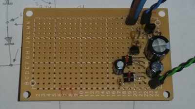 This amplifier block was designed to deliver more than 5mW into medium impedance headphones.
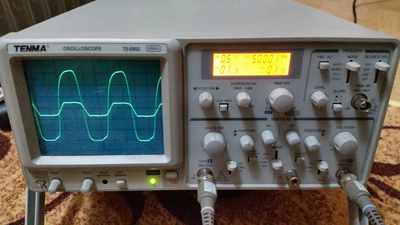
I measured the DC resistance of a couple of some all-around headphones and they had approx. 32-80 Ohms. Then with the scope and the audio generator I measured the Vpp value at which the sound pressure was so loud that it was too painful to stay with phones over head. It was around 1.6Vpp, 1KHz sine, over DC 70 Ohms, that gave me roughly 4.6mW, so the audio power must be at least 5mW into 30 Ohms.
Knowing the wanted power, supplying voltage, I started to draw countless schematic versions and spot some values with pen over paper:
 It can be seen that before the push-pull pair there is one transistor in emitor follower configuration instead of classic design with common emitter, that's because I wanted low distortion, high input impedance and low impedance for output. Of course, I could use a common emitter loaded by a current source, but simple current source doesn't scale with the supply voltage, things eventually gets too complicated beyond my scope, therefore I'm happy with that emitter follower instead of a simple common emitter loaded by resistor.
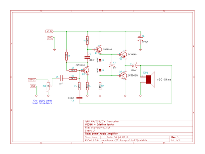 The high level description of this amplifier could be resumed as one voltage amplifier formed by Q3, a current amplifier formed by Q1 and another current amplifier formed from push pull pair Q2-Q4, also a negative feedback loop provided by C6,R5,R4.
Because voltage drop across a diode changes a bit with the current flowing through it, C3 will damp those small voltage changes across D1,D2, making the circuit more stable and decreasing distortions. The diodes were carefully selected in order to provide a good balance between crossover distortions and quiescent current consumption, therefore their voltage drop is around 0.65 each for this amp. Depending of the amp. total output power, the diodes can have lower or bigger voltage drops. For example for a powerfull amplifier diodes could have 0.550V each or in case of a very low power amp. the diodes could have 0.700V each, this is related to current flow through them. For this amp. the crossover distortions starts to appear below 9V supplied voltage.
Without the feedback loop, gain of this amp. was 31dB initially and input impedance about 14.5K. The gain is given by Q3 - the voltage amplifier. That strong negative feedback will bring the gain down by 10dB, a significant amount of the input impedance, the standby hiss and distortion levels also.
The voltage scale very well across components with respect of the supplied voltage. For a more precise adjustment to the half of supplied voltage between Q2,Q4 emittors, the R1 resistor could be replaced with a multiturn pot.
Characteristics and Testing for 12V | 27° C:
GAIN
Input voltage max: 0.270 mVpp
Output voltage max @ 50 Ohms: 3.4 Vpp
Voltage Gain: 12.6
Gain With Feedback: 22dB
Gain Without Feedback: 31dB
Beta of Transistors
2N3904 - 200
2N3906 - 213
POWER
Quiescent Current: 2.2 mA
Max Current @ 50 Ohms: 12.6 mA
Max Voltage Peak-Peak @ 50 Ohms: 3.4 Vpp
Max Power Sink @ 50 Ohms: 151 mW
Max Load Power @ 50 Ohms: 29 mW
Efficiency @ 50 Ohms: 19.2%
--------------------------------
Max Current @ 8 Ohms: 17.4 mA
Max Voltage Peak-Peak @ 8 Ohms: 0.9 Vpp
Max Power Sink @ 8 Ohms: 209 mW
Max Load Power @ 8 Ohms: 12.7mW
Efficiency @ 8 Ohms: 6%
Input Impedance
Without Negative Feedback: 14.5K
With Negative Feedback: 3.375K
With Potentiometer: 770-1000 Ohms
Impedance decreases further if the supplying voltage is increased.
Frequency Response
60Hz - 20KHz the gain is flat 22dB
8-60Hz the gain increases due lower effect of the negative feedback, because the phase is not shifted through C2,C6 to 180° for lower frequencies. The C5 could be changed to a lower value (1uF-470nF) in order to suppress low frequencies more, if this is the case.
The amplifier is able to handle even higher frequencies as 20MHz, but the gain is very low, it begins to drop above 3MHz. Maybe using quality components (cap. and metallic resitors) the higher frequency response could be improved a bit.
Total Harmonic Distortion
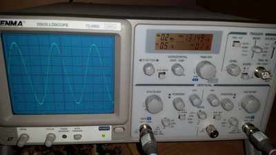
Unfortunately I cannot measure distortions because I don't have adequate equipments, but on the scope trace, the sine looks very clean, no sign of distortion at all for the naked eye, neither for my ears, but they are present I think in a very low percent. It can be seen on the peak of negative cycle that it is a bit flatten away, but mybe I didn't set the horizontal level correctly.
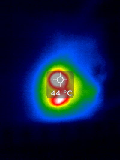
 Thermal view of push-pull transistors after 5min of full power delivered into 8 ohms
Update 5th August 2018
These days I made some research/experiments and took some conclusions. I have to change my first design orientation. Since I'm always hurrying up because I have many stuff to do, it will took too much time to design and build a "perfect" direct conversion transceiver with all kind of features builtin. I decided to make a simple version at first and then make improvements over time for other future versions. Even more, I don't have any general coverage receiver/transceiver, so I cannot wait too much anymore, therefore I have to build it as soon as possible.
These days I tried to use all kind of mixers as a product detector. Unfortunately, all kind of variants tried based on transistors failed because I have a very strong MF station nearby, 250KW from 30KM away. I cannot use transistors for mixing without filters because they go overloaded easily. Tried balanced, unbalanced, versions, no matter, they behave like diodes when a 4Vpp signal came across them.
Then I made a single balanced diode mixer and "puff" the MF station gone at the first attempt. That's because it has a high dynamic range, attenuation and many mixing garbages are canceled out by the balanced process of this type of mixer. Of course, at first I wouldn't wanted to use this kind of mixer because it has some attentuation and requires a high level of the LO in order to drive the diodes >1Vpp or >9dBm, but I realised I cannot use transistorised (including gillbert cell) mixers without band pass or notch filters.
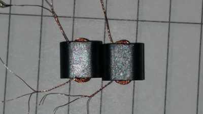
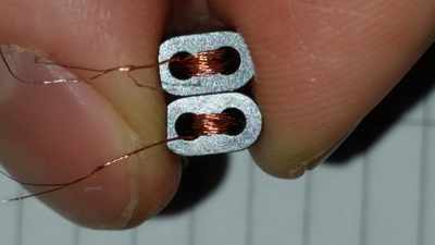
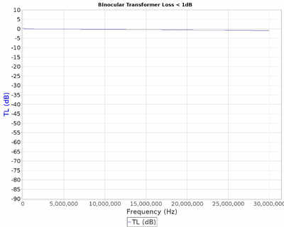
I've had very cool results with single balanced diode mixer, I wounded about 10 turns for primary and about 2x15 turns for secondary windings over a binocular core, 43 material and BAT41 diodes. I have to move it away from breadboard to PCB in order to make some measurements regarding the losses vs frequency. But I can tell that it can go down to 150KHz and up to 18MHz. I hope it has a good response up to 30MHz, we will see.
Another important thing regarding the diode mixer, it is mandatory to have a low resistive termination for all frequencies. I already anticipated that and my thougts were confirmed in "High-Performance Direct Conversion Receivers - from KK7B/QST/ARRL". Otherwise, reactive products will reflect back into mixer again and re-mixed again and so on, leading to a dirty output.
Regarding audio filter, it will be a higher order, implemented solely with LC, that's because I wanted a steep frequency response (0-3KHz)
For the receiving front end, a common base transistor stage fed through a current source will be used set to 50 Ohms, maybe some attenuation scales, protection diodes, etc.
2.5KHz 5th Order Audio Filter - 11th August 2018
As I already mentioned, I wanted a high order LC filter instead of RC + AMP because of the following reasons:
o RC filters have big attenuation, they are acting actually like voltage dividers
o RC filters needs amplification to boost again the signal at the same level (more current consumption)
o RC filters have poor frequency response without amplification
o RC filters have poor load characteristics
o LC filters have low attenuation
o LC filters are usualy made in higher order configuration without the need to reamplifying the signal (no current consumption)
o LC filters have good frequency response
o LC filters can adapt impedances
The filter used here is based upon one described by KK7B in his article in QST magazine. It is a 5th order filter, formed solely by inductors and capacitors, but there are some parasitic resistances which they should be taken into consideration also.
The input/output impedance should match the adjacent stages.
The audio filter was designed using the following tools:
o RFSim99 v1.05
o https://www-users.cs.york.ac.uk/~fisher/lcfilter


Real Measurements
 Impedance vs Frequency:
800Hz - 1100 Ohms
1500Hz - 1150 Ohms
2300Hz - 720 Ohms
2800Hz - 1480 Ohms
3200Hz - 1920 Ohms
5000Hz - 510 Ohms
8000Hz - 270 Ohms
Other Notes
o When the volume potentiometer is turned fully on, the input impedance of the filter decreases from 1K to roughly 800 Ohms due audio amplifier low input impedance. I knew that from the begining but I thought that I will use a common collector stage before the audio amp. and solve the problem. This could be a design flaw, therefore for future versions the audio amp should have higher impedance and negative feedback loop made upon a differential input pair, for example. I don't want to use now a common collector stage after the filter to "fix" this design error.
o Tried to use 7th order filter, but it didn't worked correctly - I don't know why at this moment but I suppose my breadboard leaked signals.
o Those 10nF capacitors across inductors are making that frequency roll-off more steeper, but signals greater than 10KHz are being leaked through. Therefore, they could be omitted or replaced with ones with a lower value.
Product Detector - 12th August 2018
o Today, the audio filter was mounted on PCB. It performs nicely!
o I decided that "single channel sdr receiving" feature is useless for this transceiver, so it was canceled.
o In order to test the product detector stage with antenna signals, I made a notch LC filter to knock down that local 250KW MF station.
o Made some tests again using single BJT product detector. It worked nice until evening when strong singals from powerful broadcasting stations were leaked through. Partially solved by driving the BJT harder with LO signal. I have to do more tests using different biasing and load currents, maybe make some tests with JFET or MOSFET transistors. I definitely don't want to use diode ring mixer due its poor low frequency response and high power LO driving.
Product Detector - 18th August 2018
This week I made some research regarding single BJT product detector.
Here are some quick statements:
o Transistor should work in class B (crucial importance!)
o Poor IF/RF/LO isolation
o Poor audio recovery/quality
o The BJT stage is very sensitive to input/output loads, any change in load at its ports will change its behaviour
o Good frequency response
o Simplicity
Some Operation Theory
Considering the LO voltage swing {+1V, 0V, -1V}:
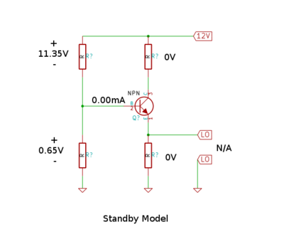 Without LO signal applied (StandBy mode) the transistor is in CutOff state, the current flows only through base resistor voltage divider. Since the lower resistor keeps Vbe at 0.65V the transistor is (mostly) turned off.
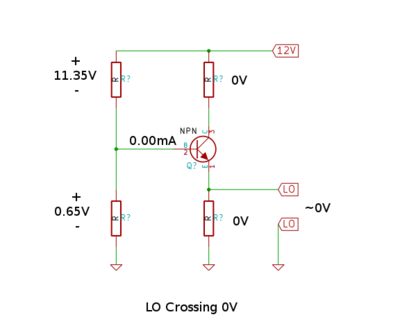 When LO AC is applied but it just reaches the 0V the BJT stage will behave mostly like the standby model.
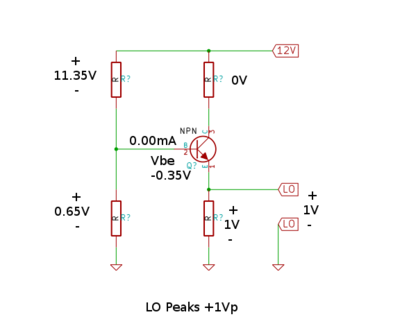 When LO peaks +1V the transistor is deeply turned off due reverse biasing of the base-emitter junction. Any positive voltage greater or equal with 0V keeps the BJT turned off (cut off state).
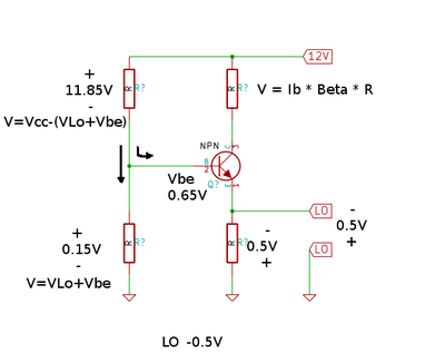
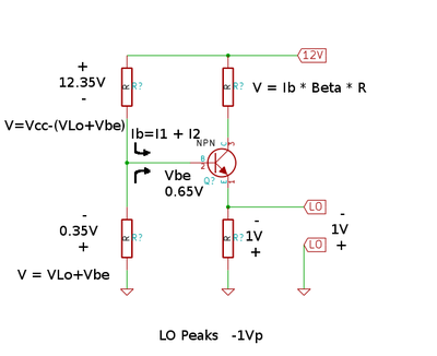 Now, when LO signal becomes more negative than 0V, the voltage across adjacent resistors changes turning the transistor on. The LO should be very low impedance in this case because Ib + Ic will flow through LO during LO negative cycle.
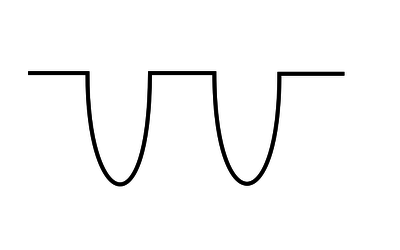
In other words, the BJT stage being class B polarised will conduct only during the LO negative cycle. The collector output waveform looks like this shape here:
 Of course, biasing resistors could be calculated for class B easily, but when RF and IF ports are loaded by adjacent stages everything gets worse. That's because the LO voltage swing over all resistors (poor LO isolation) and when a load is capacitively coupled to the RF port for example, biasing behaviour is changed.
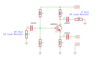
Thefore, I made the "cold" calculations, then placed the circuit onto my breadboard, loads over RF/IF ports then by trial and error I tried to get the best results on the scope while injecting LO signal and changing value of R2 resistor (tested with 1MHz).
Here is the initial BJT stage:
Product Detector - 19th August 2018
Finally, after some tweaks and a long testing period I made the schematic for the product detector.
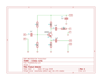 There is nothing special regarding the schematic, this type of detector its just a solution of compromise being super simple and has a good frequency response (I hope).
o The biasing resistors R2,R3 keep the transistor in class B operation, but this is valid only when LO signal is present (~0.4Vpp) and loads across RF and IF are present also. The loads are 850 ohm for IF port, 270 ohms for RF port.
o R4 set the output impedance of the stage, which is roughly 680 ohms in this case (for common emitter configuration Z-out is collector resistor).
o R6 does two things, first it adjust the output impedance from 680 to 850 ohms for audio-frequencies. And two, together with 100nF capacitor from audio filter forms a low impedance load (220 ohms) for high frequencies. In this way the transistor is kept working in class B for a wide range of LO frequencies.
o R5 just keep the output voltage low (R6/R5) and develop voltage from LO signal.
o The 1uF capacitors from I/O ports C1,C2,C3 are non-polarised type. Their values are so big because they should let low frecuencies from ELF-VLF range passing. I'm expecting that they should be poor for HF and a 100nF ceramic type should be connected in parallel with them. We will, see...
I'm expecting also high frequencies bad response due low quality of the components. Again, we will see.
Product Detector - 20 August 2018
Today I placed the BJT product detector onto the PCB, took some measurements and pictures.
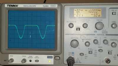
Collector Output 1
o LO signal only (no RF)
o RF closed by 470R
o 3V Swing
o BJT Class B
o 1 MHz
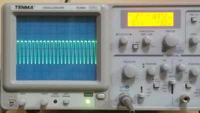
Collector Output 2
o LO signal only (no RF)
o RF port closed by 470R
o 3V Swing
o BJT Class B
o 1 MHz
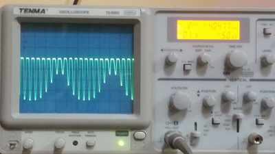
Collector Output 3
o LO signal 1.000MHz
o RF signal 1.100MHz, series 470R
o 3V Swing
o BJT Class B
Collector Output vs Audio Recovery
o Collector 1.6Vpp
o Audio recovered after filter 10mVpp
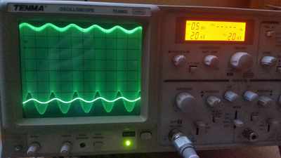
Recovered Audio
o Poor quality
o 600mVpp
o 1.000MHz + 1.001MHz = 1KHz audio
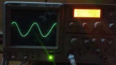
RF Port Leak
o Poor LO isolation at RF port
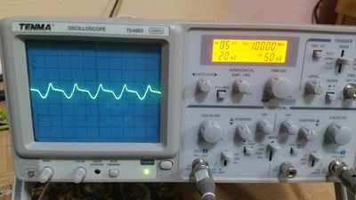
Conversion Table
o 470R in series with generator at RF port
o RF Vin read after generator and before 470R
| Freq |
RF Vin |
LO Vin |
Audio Vout |
| 100 KHz |
120 mVpp |
400 mVpp |
140 mVpp |
| 500 KHz |
200 mVpp |
500 mVpp |
180 mVpp |
| 1 MHz |
200 mVpp |
500 mVpp |
180 mVpp |
| 2 MHz |
200 mVpp |
500 mVpp |
180 mVpp |
| 3.5 MHz |
190 mVpp |
520 mVpp |
160 mVpp |
| 5 MHz |
180 mVpp |
540 mVpp |
150 mVpp |
| 7 MHz |
180 mVpp |
540 mVpp |
140 mVpp |
| 10 MHz |
180 mVpp |
520 mVpp |
120 mVpp |
| 14 MHz |
200 mVpp |
500 mVpp |
80 mVpp |
| 18 MHz |
230 mVpp |
500 mVpp |
50 mVpp |
Other Notes
o While varying the power supply voltage the amplification was impacted mostly. Class B polarisation was afected just a bit, therefore I think there is no need to regulate the power supply for this product detector.
o I was expecting the high frequency poor response, because of the quality and layout of the components. A good improvement could be obtained by using metal film resistors, RF transitor and maybe SMD techology.
o The detector is able to pick weak signals from antenna without any help of amplification. Tested around 130KHz-14MHz, above this range the audio output is very low.
o Better AM rejection with LO 0.7Vpp tested at 3.7MHz.
o Current consumption is around 5.2mA.
o Total current consumption 7.4mA (audio + product detector).
Next, I have to build an RF amplifier composed from common base fed by a current source followed by a common collector stage. The RF gain would be around 40-50dB, current consumption around 10mA. Then I have to check if the receiver needs an AGC circuit.
45dB 50R RF Amplifier - 24th August 2018
o The RF amplifier is formed by a common base followed by common collector, the amplification gain is around 45dB for 100KHz-30MHz. Tried to load the common base with a current source but the amplification was so big (55dB) that any change in temperature or other external factors left the amplifier with wrong voltage offset. Therefore, the common base amplifier is loaded by 8K2 resistor now.
o Regarding the AGC implementation, I tested JFET VCR (voltage controlled resistor) it worked nicely. Maybe a diff pair should be taken into consideration too.
o Unfortunately, I didn't made any AGC implementation due space limitation on PCB.
The RF amplifier schematic:
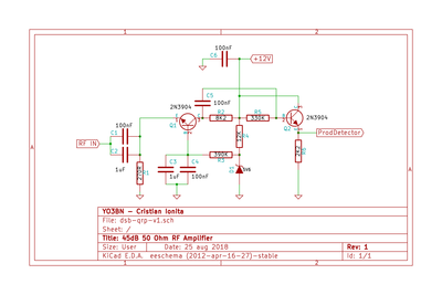 As a short description, we have Q1 acting as a constant low input impedance (approx. 50 Ohms RF) and voltage amplifier. This stage has a gain about 45dB over entire 100KHz-30MHz frequency range. But the output impedance is very high, therefore it cannot fed any other stage than a current amplifer, it is followed by Q2 in this way.
As the input impedance for RF is a function of Ie current through Q1, this could be changed by varying the supply voltage, therefore in order to keep input impedance approximately constant D1 is regulating the voltage applied to base resistor R3 trying to keep the current constant for Ib and Ie respectively.
The RF Input Impedance @ 12V 30°C:
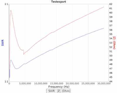
The RF Gain table:
| FREQ |
Vin |
Vout |
Gain |
| 100 KHz |
5 mVpp |
1.1 Vpp |
46.8 dB |
| 200 KHz |
5.5 mVpp |
1.2 Vpp |
46.7 dB |
| 400 KHz |
6 mVpp |
1.2 Vpp |
46.0 dB |
| 600 KHz |
6 mVpp |
1.2 Vpp |
46.0 dB |
| 800 KHz |
6 mVpp |
1.2 Vpp |
46.0 dB |
| 1 MHz |
6 mVpp |
1.2 Vpp |
46.0 dB |
| 2 MHz |
5.5 mVpp |
1.2 Vpp |
46.7 dB |
| 4 MHz |
5 mVpp |
0.9 Vpp |
45.1 dB |
| 6 MHz |
4 mVpp |
0.6 Vpp |
43.5 dB |
| 8 MHz |
3 mVpp |
0.56 Vpp |
45.4 dB |
| 10 MHz |
2.4 mVpp |
0.48 Vpp |
46.0 dB |
| 12 MHz |
1.8 mVpp |
0.42 Vpp |
47.3 dB |
| 14 MHz |
1.5 mVpp |
0.38 Vpp |
48.0 dB |
| 16 MHz |
1.2 mVpp |
0.34 Vpp |
49.0 dB |
| 18 MHz |
1 mVpp |
0.31 Vpp |
49.8 dB |
| 20 MHz |
1 mVpp |
0.3 Vpp |
49.5 dB |
| 24 MHz |
0.8 mVpp |
0.26 Vpp |
50.2 dB |
| 27 MHz |
0.8 mVpp |
0.25 Vpp |
49.9 dB |
| 30 MHz |
1 mVpp |
0.24 Vpp |
47.6 dB |
Other Notes
o Unfortunately, with such RF amplifier, strong AM stations are leaking through regardless the LO frequency. I was expected this but the receiver now is useless without attenuators and sharp band pass filters.
o Also, the weakest link in the chain is the product detector which is prone to AM detection.
o Some of LO signal is leaked at the RF (antenna) input, also due product detector low isolation.
o The overall receiver current consumption is around 12.6mA fed only with LO signal.
Product Detector II - 29 August 2018
As the receiver became useless with that amplifier, the BJT product detector was ripped out from the PCB being replaced by passive simple balanced diode mixer.
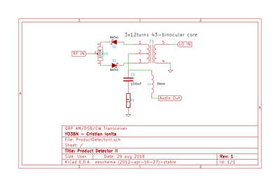 The heart of this product detector is the phasing transformer and its afferent diodes. The transformer is made of 3x12 twisted turns upon a binocular core of 43 material. It works in a high impedant load, about 1K because I want to drive diodes with less LO power, but I'm expecting poor quality in this case. The product frequencies ends up into 1K load, C1 R1 for frequencies greater than 3KHz, and the lower audio frequencies goes through L1 to audio filter which has 850R-1K input impedance. The potentiometer RV1 is used to finely adjust the balance of this product detector, lowering chances of LO leaks toward antenna and AM detection. Of course, while changing the LO frequency, the parasitic reactance between mixer components is also changing, therefore the balance of the mixer is in turn disturbed especially for high frequencies above 5MHz.
After the scrapping of that BJT product detector, I found that the Q1 in the RF amplifier could be very easily overloaded by strong signals, therefore the need of using sharp band pass filters became obvious. Also, without that BJT the audio volume was also reduced, therefore another amplifying stage should be introduced into RF or audio chain in future designs, or maybe it can be improved by raising LO voltage.
The current consumption now is 6.62mA with or without LO signal.
Unfortunately, I didn't had enough time to measure the frequency response, but using signals from antenna the mixer is able to pick up signals from 135KHz-14MHz, on generator it goes over 50MHz.
Audio Preamplifier - 9th September 2018
In the last days I didn't had enough time to continue my work. As I already said above, the audio volume now is lower without that BJT product detector, therefore I made a simple common emitter amplifier in order to boost the audio.
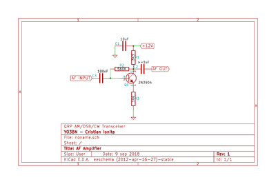 This circuit is placed between volume potentiometer RV1 and R4 from audio amplifier section and was designed to have a high input impedance (100R * Beta 200 = 20K - Negative Feedback R) and roughly 3K output. The audio level now is better than sufficient and the receiver visible lacks of AGC.
The current consumption now is 8.3mA @ 12V for entire receiver circuit without DDS.
Complete Receiver 8.5mA @ 12V - 26th September 2018
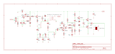 Characteristics:
o Quiescent Current Consumption: 8.3mA @ 12V
o RF Input Impedance: 56 ohms @ 500KHz-30MHz
o AF Output Impedance: 30 ohms
o AF Output Power: 29mW @ 50 ohms
Notes:
o RF input impedance and biasing current for Q2 could be adjusted from D4, R4 and R7.
o D3 and D5 should be carefully selected for lowest current consumption and low cross-over distortion for audio push-pull amplifier.
o Frequency response of T1 should be measured for future projects.
o Frequency response of the entire receiver depends upon RF amplifier Q1, Q2, product detector transformer T1, and LO signal.
o Frequency response and gain measured to RF amp. Q1, Q2 are not 100% correct. My scope sensitivity become inaccurate above 7MHz.
o Inserting Q7 to boost the audio level also introduce positive feedback from antenna to audio output, therefore using long and non-grounded wires could lead to auto-oscillations.
o Audio filter could be optional.
o Optional AGC circuit.
Kicad files here.
Designing the DDS Circuit - 26th September 2018
HW & SW Objectives:
o Low power consumption
o Display On/Off/Profile
o Display Light On/Off/Profile
o CPU Idle Sleep
o Peripherals Disabling
o Voltage Monitoring
o Rotary Incremental Encoder + Push Button
o Menu + Service Menu
o Frequency Memories + Band Labels
o Programmable Scanning
o Configurable Stepping
o CW Configurable Shift
o Dual Watch / Triple Watch
o Rx/Tx VFO Split
o RTTY Encoding/Decoding (future versions)
o Beacon Capability
o Bootloader for FW upgrade
o Using LM317 instead of 7805 (7805 quiescent current = approx. 6mA, which is too much)
o Using AD9834 DDS Integrated Circuit
o Using Low Pass Filter
o Using RF Amplifiers; Output Impedance < 1000R
Other Notes:
o Atmega1284 current consumption for active 1MHz internal RC clock is around 600uA, which IMHO is very good. Maybe I have to raise the clock a bit changing the prescaling.
o 2x16 Hitachi Display current consumption for active display and backlight is around 7mA. I think is too much, but I have no choice for the moment. For future versions, an 84x84 Nokia display could be a good candidate.
o During the research & development stages the DDS controller will be my Atmega Dev.Board v2.
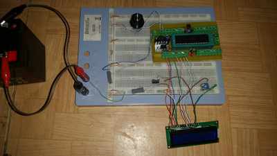
AD9834 Circuit - 9th October 2018
Unfortunately, things are going very slow, I always had other important stuff to do. But anyway these weeks I built almost entire DDS circuitry, some kicad libs and testing software for MCU.
First, I have designed the following DDS circuit:
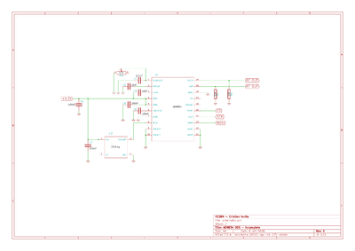 After some tests I took the following conclusions:
* It didn't worked at the first attempt because of 75MHz TXO lower clock output. The TXO is rated to Vcc max 3V6, therefore I was forced to raise the Vcc from 3V3 to 4V3 in order get a higher output and cock the AD9834. The TXO is ASDMB-75.000MHZ-XY-T ABRACON 10ppm accuracy but seem to be quite unstable though.
* The RF output is a differential output.
* The RV1 at pin 1 is used to set Iout over 220R resistors, RF output respectively. The magnitude of Iout is 18 times larger than Iset. So, on this pin a constant voltage source of 1.15V is used to set Iset through RV1. According to datasheet formula, we have Iout = 18 x FSADJUST/Rset, where FSADJUST = 1.15 nominal; Rset is RV1 resistance.
* Setting the current at pin 1 using the datasheet formula is only true for lower frequencies, above 1MHz the output decreases considerably. For lower frequencies the RF output can be roughly 2Vpp, while for higher frequencies like 25MHz the output is less than 200mVpp.
* In order to make the RF output stable across entire range I have developed an automated HW & SW solution to set the Iset at pin 1 using an open collector NPN bjt and an 8bit MCP4901 DAC controlled by MCU. Then Iset can be set from 10uA to 1.2mA in 256 steps. The software will set the Iset first and then the DDS frequency.
* I have to find a solution ragarding the amplfying stages of the differential RF output before to take the decision to use single ended output, I'm thinking to a diff pair, or directly a current mirror.
* Above 18MHz the output sinewave becomes a bit distorted and very ugly above 25MHz. I hope to fix this issue with a low pass filter.
AD9834 Circuit + MCP4901 DAC
In order to keep RF output roughly constant, Iset at FSADJUST (pin 1) of AD9834 need to be dynamically adjusted. For this purpose I used a super low power 8bit DAC - MCP4901- which draws around 200uA without load. A hardcoded table will be implemented in software containing frequency ranges and their DAC value. The DAC is controlled via SPI bus, then the voltage given by the DAC will drive an open collector NPN transistor Q1 in schematic, in order to set Iset.
* The Iset current range can be set from 10uA to 1.2mA in 256 not-so-linear steps. The linearity will be corrected by software, it can even correct the gain vs freq. non-linearity of the RF amplifiers.
* The software have to set first the DAC value and then the frequency due C9 delay which should provide a smooth transition.
* It will be nice to let the user to modify the freq-dac table from menu.
 Next, I have to implement the voltage source for the DDS and for the digital part, a source with very low quiescent current consumption: max. 1mA. I think it will be based on LM317.
LM317 Voltage Source - 14th October 2018
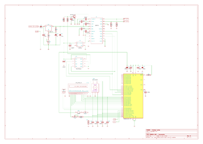
Since I wanted a low quiescent voltage source, instead of wasting around 6mA using a 7805 regulator I have designed a voltage source using the LM317L available in TO-92 package. LM317L is capable to deliver around 100mA of current, being by far enough for the entire DDS + MCU current consumption.
First, I have to recapitulate how LM317 works. It is a three terminal IC, which operates in "floating mode" that means it doesn't need a GND connection to work. However, used in voltage regulation configuration it should have GND connection through a resistor.
The datasheet specifies four important aspects:
1. The LM317 circuit will raise the voltage at OUTPUT pin by 1.25V higher than ADJUST pin voltage.
2. The current at ADJUST pin is roughly 50uA.
3. The minimum load current should be 3.5mA typical.
4. Headroom voltage, Vi - Vo = 3V
Explaining the datasheet figure 9 for voltage regulator:
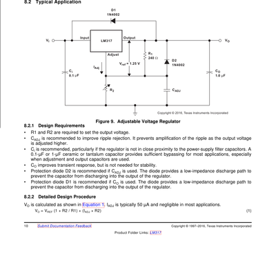 While the voltage across R1 is kept nailed to 1.25V (between OUTPUT and ADJUST pins) the rest of voltage (Vout - 1.25V) drops over R2. Also, to voltage dropped over R2 is added Iadj, the Iadj is roughly 50uA.
Explaining the datasheet equation: Vo = Vref(1 + R2/R1) + (Iadj * R2)
Let's say that voltage drop across R1 is represented by Vr1, same for R2, Vr2.
Using Kirchhoff Voltage Law, we have Vo = Vr1 + Vr2
The Vr1 equals Vref, 1.25V.
Voltage drop across R2 is defined as (Iadj + Ir1) multiplied by R2, so Vo = Vref + R2(Iadj + Ir1)
Current through R1 is Vref/R1, then Vo = Vref + R2(Iadj + Vref/R1)
Vo = Vref + (R2 * Iadj) + (Vref * R2)/R1
Vo = Vref + Vref*(R2/R1) + (Iadj * R2)
Vo = Vref(1 + R2/R1) + (Iadj * R2)
Simple as that :)
Now, for my design I choosed as a simple rule that Ir1 to be twice greater than Iadj, that means the quiescent current will be 3 * Iadj = 150uA, which is reasonable in my opinion. Then, R1 could be found by dividing Vref to 2*Iadj => R1 = 1.25V / 100uA => R1 = 12500 ohms, approx. 12K
Then, I wanted Vo to be adjustable around 3V to 5V, therefore for the lower voltage 3V the Vr2 = Vo - Vref <=> Vr2 = 3V - 1.25V => Vr2 = 1.75V. The current through R2 is Ir1 + Iadj, 150uA, thus R2 = 1.75V / 150uA = 11666 ohms, approx. 12K.
Calculating R2 for 5V: Vr2 = Vo - Vref = 5V - 1.25V = 3.75V. The current is 150uA, therefore the R2 = 3.75V / 150uA = 25000 ohms, approx 22K.
I had the two resistors now, R1 = 12K; R2 = {12K,25K}. So, I can split the R2 into 12K + 10K potentiometer in order to cover the 12K-22K range, 3-5V respectively.
After the breadboarding, I've found that I was close enough, the voltage can be adjusted between 3V-4.5V, so I have replaced R2 by 15K + 10K POT, then the voltage range was moved higher to 3.5V to 5.0V and I was pretty happy with the latest result.
Furthermore, the D1 and D2 are used to protect the LM317 circuit against Vin shortcircuit. Since, Co and Cadj could be charged when a Vin shortcircuit occurs, the diodes provide a low impedance discharge path for these capacitors. Thus Co is discharged through D1, Cadj is discharged via D2.
In my design I will not add those diodes, but only a polarity protection diode, which will protect against Vi shorts also. The headroom voltage is increased then to 3.7V, therefore for 5V, the Vin should be 5V + 3.7V = 8.7V.
Depending of DDS + MCU current draw (I hope approx. 30mA), the power dissipated over LM317L could be somewhere around <200mW @ 12V.
For lower power consumption a switched voltage regulator can be taken into consideration.
I have updated the schematic also:
 Next I have to do:
- Build the prototype DDS + MCU module
- Make a low pass filter
- Design RF amplifiers
- MCU ADC wiring and divider
DDS Prototype Part 1 - Update 22nd October 2018
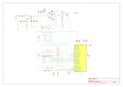
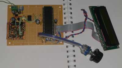 I've been mega disappointed! After placing all important components like MCU, LCD, DAC, LM317LZ on the test PCB I was so impatient to add the AD9834 and the clock too. First power up, the overall current sunk was around 17mA with MCU in running state, LCD + backlight on, DDS with minimum output, which was a very impressive result, but after I set the output of AD9834 to full scale, the current consumption raised to 40mA, only AD9834 and its clock ate around 37mA @ 4.3V. Almost all current was dropped over those two 220R resistors from AD RF output. Therefore I've been disappointed. I tried to change them with 1K, but the output was very distorted so I have restored back the 220R resistors. Even more, I tied directly to ground the IOUTB because this improved the output waveform while the current consumption remained the same.
I have to redesign the voltage regulator for future hardware versions. I will use a switching DC/DC buck voltage regulator, hoping that I can save more than 20mA in this variant, but I'm worried about switching noise in this case.
I made some minor modification to the schematic also.
 Next I have to:
- Make a low pass filter
- Design RF amplifiers
- MCU ADC wiring and divider for supply voltage monitoring
Finished DDS - 10th November 2018
I finished the DDS amplifying circuitry some weeks ago and meanwhile I have enjoyed very much MF and HF listening. Finally, now I have time to write the changes down here. Unfortunately, I rushed through this stage too, therefore I didn't made it as I really wanted.
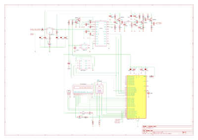 Looking on the schematic, the transistor Q2 is acting as high input impedance stage and current amplifier for the following low pass filter C27, L1, C26. The filter is loaded by R14. Unfortunately, I do not remember exactly the value of L1. Then, the voltage is amplified by Q4. The C29 helps the linearity of RF amplification, if C29 is omitted the amplifications decreases above 10MHz. Q3 is a high impedance input stage, low impedance output stage.
Unfortunately, I didn't had much time to experiment/design better filters. The DDS seems to be rich in harmonics, it should be filtered more better in future versions, using padded filters and clean amplification.
The entire DDS module draw around 40mA @ 12V.
The output RF voltage loaded by 1K resistor is roughly 3Vpp if I remember correctly. Maybe I should make the measurements again and make a graph.
TODO:
- ADC for voltage monitoring
- ADC keypad
- Buffer stages for Rx / Tx ?
Update - December 30th 2018 - Voltmeter, Field Testing and Fixes
 The voltmeter was implemented in hardware and software meanwhile. Now the battery voltage is displayed on the left coner onto 2x16 LCD screen. For the hardware part a voltage divider R18, R19, was designed to scale down a maximum of 20Vcc to 2.56V ADC reference, while maintaining an equivalent thevenin impedance of 8.7K (less than 10K Ohms is specified by ATmega1284 datasheet) and a low level of quiescent current consumption (153uA @ 12V).
Notice, there is no trimer pot for voltage divider to adjust the tolerances. Since a trimer is a bit bulky, heavy and pricey, the ratio of divider + tolernaces will be corrected by software.
The D2, 5V6 zener diode is a protection for MCU since divider is connected directly to VCC bypassing the protecton diode D1, therefore the zener should short reverse voltages to GND and trim large spikes. The MCU also provide a protection diode inside, but for safety reasons an external diode was added.
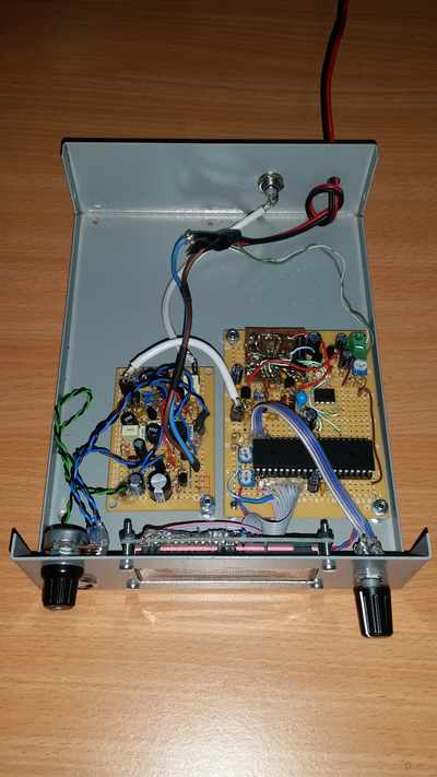
The receiver was mounted into a case together with the DDS, MCU and LCD. After a long period of testing meanwhile it showed poor AM broadcasting rejection, magnetic field pick up and lack of RF level amplification while using small loop antennas.
The AM Broadcasting Rejection
Unfortunately, this was a serious design flaw. First, the major issue here was Q2 buffer stage in the receiver schematic. It behaved totally unlinear when was loaded by mixer, even with 1K loading at the IF port. Strong signals in the antenna are amplified up to 8Vpp by the Q1 stage, then the second stage Q2 cannot drive correctly the 1K load seen at the IF port when the mixer diodes are closed by LO.
To fix this, another buffer stage was added in order to further lower the impedance for the mixer Q8, increasing the current consumption too. The second buffer fed the mixer through a 390 Ohms metal film resistor now R20, thus to prevent strong loading provided by the mixer and introduce some degree of attenuation too.
The second problem was the mixer, diplexer, audio filter which all were designed for 1K loading. Diodes are not so happy when they are dealing with high impedances, in this case being prone to intermodulation. Here, the single balanced mixer was changed to a double balanced one increasing the audio volume a bit and a shunt of 120R R22 was added to IF port to increase load for diodes, also decreasing the audio volume a bit.
Another resistor of 340R metal film (2x680R) was placed between DDS output and mixer LO input, R21. Thus, to prevent strong loading to the DDS output stage by mixer and normalize switching voltages across diodes.
After all these changings and adjustments, the receiver is more quiet. While antenna is disconnected the internal receiver noise is mostly the same on all frequencies with or without LO signal driving the diode mixer. The AM broadcast rejection was improved a lot now. The only thing for further improving this is to implement an AGC circuit.
Magnetic Field Pick Up
The receiver is able to pick some hum noise, pop and clicks apparently without any reason. I've found that inductors used in the audio filter are very prone to microphonics and magnetic field detection since they are open field inductors. This issue could be easily fixed by using closed field inductors for the audio filter for future versions.
Lack of RF Level
During portable operations using small loop antenna the RF level seemed to be too low directly impacting the audio volume. On big antennas there is plenty of audio volume, but since small loops have attenuation the RF level is also low. The background noise in the receiver is mostly the audio stage noise. Therefore, a common emitter and an AGC circuit should be placed between the two buffers stages in front of diode mixer, further increasing AM rejection by the RF limitation for mixer. Or much more gain and AGC implemented at audio level.
Latest Schematics
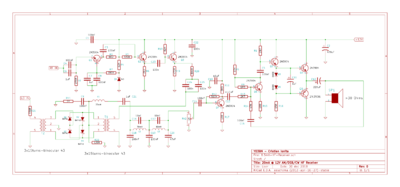
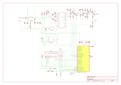 Kicad files here.
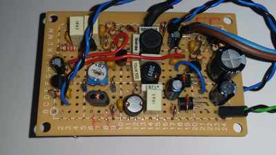
Some Photos


Other Notes
- The receiver was tested with antenna signals from 10KHz up to 18.1MHz.
- Above 13MHz, the overall gain decreases, also the LO signal becomes mostly triangular (according to my scope).
- Below 10KHz the mixer transformers does not have a good transfer with the actual LO power, but it can be pushed down to ~3KHz with poor results.
- Below 16KHz the LO leaks through audio filter, therefore it can be heard in background.
- The overall current consumption is around 66mA @ 12V due Q8 buffer stage in receiver schematic.
- In the future the audio stage should have a differential amplifier to take negative feedback.
- In the future the mixer should be built around a differential transistor pair in order to lower the current consumption, decreasing the RF/LO port power needed by diode mixer.
- Another stage of at least 20dB RF gain is needed in the future.
- AGC stages for the future.
- The BNC connector may be placed on the front panel.
To Be Continued


This amplifier block was designed to deliver more than 5mW into medium impedance headphones. I measured the DC resistance of a couple of some all-around headphones and they had approx. 32-80 Ohms. Then with the scope and the audio generator I measured the Vpp value at which the sound pressure was so loud that it was too painful to stay with phones over head. It was around 1.6Vpp, 1KHz sine, over DC 70 Ohms, that gave me roughly 4.6mW, so the audio power must be at least 5mW into 30 Ohms. Knowing the wanted power, supplying voltage, I started to draw countless schematic versions and spot some values with pen over paper:
It can be seen that before the push-pull pair there is one transistor in emitor follower configuration instead of classic design with common emitter, that's because I wanted low distortion, high input impedance and low impedance for output. Of course, I could use a common emitter loaded by a current source, but simple current source doesn't scale with the supply voltage, things eventually gets too complicated beyond my scope, therefore I'm happy with that emitter follower instead of a simple common emitter loaded by resistor.
The high level description of this amplifier could be resumed as one voltage amplifier formed by Q3, a current amplifier formed by Q1 and another current amplifier formed from push pull pair Q2-Q4, also a negative feedback loop provided by C6,R5,R4. Because voltage drop across a diode changes a bit with the current flowing through it, C3 will damp those small voltage changes across D1,D2, making the circuit more stable and decreasing distortions. The diodes were carefully selected in order to provide a good balance between crossover distortions and quiescent current consumption, therefore their voltage drop is around 0.65 each for this amp. Depending of the amp. total output power, the diodes can have lower or bigger voltage drops. For example for a powerfull amplifier diodes could have 0.550V each or in case of a very low power amp. the diodes could have 0.700V each, this is related to current flow through them. For this amp. the crossover distortions starts to appear below 9V supplied voltage. Without the feedback loop, gain of this amp. was 31dB initially and input impedance about 14.5K. The gain is given by Q3 - the voltage amplifier. That strong negative feedback will bring the gain down by 10dB, a significant amount of the input impedance, the standby hiss and distortion levels also. The voltage scale very well across components with respect of the supplied voltage. For a more precise adjustment to the half of supplied voltage between Q2,Q4 emittors, the R1 resistor could be replaced with a multiturn pot. Characteristics and Testing for 12V | 27° C: GAIN Input voltage max: 0.270 mVpp Output voltage max @ 50 Ohms: 3.4 Vpp Voltage Gain: 12.6 Gain With Feedback: 22dB Gain Without Feedback: 31dB Beta of Transistors 2N3904 - 200 2N3906 - 213 POWER Quiescent Current: 2.2 mA Max Current @ 50 Ohms: 12.6 mA Max Voltage Peak-Peak @ 50 Ohms: 3.4 Vpp Max Power Sink @ 50 Ohms: 151 mW Max Load Power @ 50 Ohms: 29 mW Efficiency @ 50 Ohms: 19.2% -------------------------------- Max Current @ 8 Ohms: 17.4 mA Max Voltage Peak-Peak @ 8 Ohms: 0.9 Vpp Max Power Sink @ 8 Ohms: 209 mW Max Load Power @ 8 Ohms: 12.7mW Efficiency @ 8 Ohms: 6% Input Impedance Without Negative Feedback: 14.5K With Negative Feedback: 3.375K With Potentiometer: 770-1000 Ohms Impedance decreases further if the supplying voltage is increased. Frequency Response 60Hz - 20KHz the gain is flat 22dB 8-60Hz the gain increases due lower effect of the negative feedback, because the phase is not shifted through C2,C6 to 180° for lower frequencies. The C5 could be changed to a lower value (1uF-470nF) in order to suppress low frequencies more, if this is the case. The amplifier is able to handle even higher frequencies as 20MHz, but the gain is very low, it begins to drop above 3MHz. Maybe using quality components (cap. and metallic resitors) the higher frequency response could be improved a bit. Total Harmonic Distortion Unfortunately I cannot measure distortions because I don't have adequate equipments, but on the scope trace, the sine looks very clean, no sign of distortion at all for the naked eye, neither for my ears, but they are present I think in a very low percent. It can be seen on the peak of negative cycle that it is a bit flatten away, but mybe I didn't set the horizontal level correctly.
Thermal view of push-pull transistors after 5min of full power delivered into 8 ohms


Impedance vs Frequency: 800Hz - 1100 Ohms 1500Hz - 1150 Ohms 2300Hz - 720 Ohms 2800Hz - 1480 Ohms 3200Hz - 1920 Ohms 5000Hz - 510 Ohms 8000Hz - 270 Ohms
Without LO signal applied (StandBy mode) the transistor is in CutOff state, the current flows only through base resistor voltage divider. Since the lower resistor keeps Vbe at 0.65V the transistor is (mostly) turned off.
When LO AC is applied but it just reaches the 0V the BJT stage will behave mostly like the standby model.
When LO peaks +1V the transistor is deeply turned off due reverse biasing of the base-emitter junction. Any positive voltage greater or equal with 0V keeps the BJT turned off (cut off state).

Now, when LO signal becomes more negative than 0V, the voltage across adjacent resistors changes turning the transistor on. The LO should be very low impedance in this case because Ib + Ic will flow through LO during LO negative cycle. In other words, the BJT stage being class B polarised will conduct only during the LO negative cycle. The collector output waveform looks like this shape here:
Of course, biasing resistors could be calculated for class B easily, but when RF and IF ports are loaded by adjacent stages everything gets worse. That's because the LO voltage swing over all resistors (poor LO isolation) and when a load is capacitively coupled to the RF port for example, biasing behaviour is changed. Thefore, I made the "cold" calculations, then placed the circuit onto my breadboard, loads over RF/IF ports then by trial and error I tried to get the best results on the scope while injecting LO signal and changing value of R2 resistor (tested with 1MHz). Here is the initial BJT stage:

There is nothing special regarding the schematic, this type of detector its just a solution of compromise being super simple and has a good frequency response (I hope). o The biasing resistors R2,R3 keep the transistor in class B operation, but this is valid only when LO signal is present (~0.4Vpp) and loads across RF and IF are present also. The loads are 850 ohm for IF port, 270 ohms for RF port. o R4 set the output impedance of the stage, which is roughly 680 ohms in this case (for common emitter configuration Z-out is collector resistor). o R6 does two things, first it adjust the output impedance from 680 to 850 ohms for audio-frequencies. And two, together with 100nF capacitor from audio filter forms a low impedance load (220 ohms) for high frequencies. In this way the transistor is kept working in class B for a wide range of LO frequencies. o R5 just keep the output voltage low (R6/R5) and develop voltage from LO signal. o The 1uF capacitors from I/O ports C1,C2,C3 are non-polarised type. Their values are so big because they should let low frecuencies from ELF-VLF range passing. I'm expecting that they should be poor for HF and a 100nF ceramic type should be connected in parallel with them. We will, see... I'm expecting also high frequencies bad response due low quality of the components. Again, we will see.


 As a short description, we have Q1 acting as a constant low input impedance (approx. 50 Ohms RF) and voltage amplifier. This stage has a gain about 45dB over entire 100KHz-30MHz frequency range. But the output impedance is very high, therefore it cannot fed any other stage than a current amplifer, it is followed by Q2 in this way.
As the input impedance for RF is a function of Ie current through Q1, this could be changed by varying the supply voltage, therefore in order to keep input impedance approximately constant D1 is regulating the voltage applied to base resistor R3 trying to keep the current constant for Ib and Ie respectively.

 The heart of this product detector is the phasing transformer and its afferent diodes. The transformer is made of 3x12 twisted turns upon a binocular core of 43 material. It works in a high impedant load, about 1K because I want to drive diodes with less LO power, but I'm expecting poor quality in this case. The product frequencies ends up into 1K load, C1 R1 for frequencies greater than 3KHz, and the lower audio frequencies goes through L1 to audio filter which has 850R-1K input impedance. The potentiometer RV1 is used to finely adjust the balance of this product detector, lowering chances of LO leaks toward antenna and AM detection. Of course, while changing the LO frequency, the parasitic reactance between mixer components is also changing, therefore the balance of the mixer is in turn disturbed especially for high frequencies above 5MHz.
After the scrapping of that BJT product detector, I found that the Q1 in the RF amplifier could be very easily overloaded by strong signals, therefore the need of using sharp band pass filters became obvious. Also, without that BJT the audio volume was also reduced, therefore another amplifying stage should be introduced into RF or audio chain in future designs, or maybe it can be improved by raising LO voltage.
The current consumption now is 6.62mA with or without LO signal.
Unfortunately, I didn't had enough time to measure the frequency response, but using signals from antenna the mixer is able to pick up signals from 135KHz-14MHz, on generator it goes over 50MHz.
 This circuit is placed between volume potentiometer RV1 and R4 from audio amplifier section and was designed to have a high input impedance (100R * Beta 200 = 20K - Negative Feedback R) and roughly 3K output. The audio level now is better than sufficient and the receiver visible lacks of AGC.
The current consumption now is 8.3mA @ 12V for entire receiver circuit without DDS.

 Characteristics:
o Quiescent Current Consumption: 8.3mA @ 12V
o RF Input Impedance: 56 ohms @ 500KHz-30MHz
o AF Output Impedance: 30 ohms
o AF Output Power: 29mW @ 50 ohms
Notes:
o RF input impedance and biasing current for Q2 could be adjusted from D4, R4 and R7.
o D3 and D5 should be carefully selected for lowest current consumption and low cross-over distortion for audio push-pull amplifier.
o Frequency response of T1 should be measured for future projects.
o Frequency response of the entire receiver depends upon RF amplifier Q1, Q2, product detector transformer T1, and LO signal.
o Frequency response and gain measured to RF amp. Q1, Q2 are not 100% correct. My scope sensitivity become inaccurate above 7MHz.
o Inserting Q7 to boost the audio level also introduce positive feedback from antenna to audio output, therefore using long and non-grounded wires could lead to auto-oscillations.
o Audio filter could be optional.
o Optional AGC circuit.
Kicad files here.

 After some tests I took the following conclusions:
* It didn't worked at the first attempt because of 75MHz TXO lower clock output. The TXO is rated to Vcc max 3V6, therefore I was forced to raise the Vcc from 3V3 to 4V3 in order get a higher output and cock the AD9834. The TXO is ASDMB-75.000MHZ-XY-T ABRACON 10ppm accuracy but seem to be quite unstable though.
* The RF output is a differential output.
* The RV1 at pin 1 is used to set Iout over 220R resistors, RF output respectively. The magnitude of Iout is 18 times larger than Iset. So, on this pin a constant voltage source of 1.15V is used to set Iset through RV1. According to datasheet formula, we have Iout = 18 x FSADJUST/Rset, where FSADJUST = 1.15 nominal; Rset is RV1 resistance.
* Setting the current at pin 1 using the datasheet formula is only true for lower frequencies, above 1MHz the output decreases considerably. For lower frequencies the RF output can be roughly 2Vpp, while for higher frequencies like 25MHz the output is less than 200mVpp.
* In order to make the RF output stable across entire range I have developed an automated HW & SW solution to set the Iset at pin 1 using an open collector NPN bjt and an 8bit MCP4901 DAC controlled by MCU. Then Iset can be set from 10uA to 1.2mA in 256 steps. The software will set the Iset first and then the DDS frequency.
* I have to find a solution ragarding the amplfying stages of the differential RF output before to take the decision to use single ended output, I'm thinking to a diff pair, or directly a current mirror.
* Above 18MHz the output sinewave becomes a bit distorted and very ugly above 25MHz. I hope to fix this issue with a low pass filter.
 Next, I have to implement the voltage source for the DDS and for the digital part, a source with very low quiescent current consumption: max. 1mA. I think it will be based on LM317.
 While the voltage across R1 is kept nailed to 1.25V (between OUTPUT and ADJUST pins) the rest of voltage (Vout - 1.25V) drops over R2. Also, to voltage dropped over R2 is added Iadj, the Iadj is roughly 50uA.
Explaining the datasheet equation: Vo = Vref(1 + R2/R1) + (Iadj * R2)
Let's say that voltage drop across R1 is represented by Vr1, same for R2, Vr2.
Using Kirchhoff Voltage Law, we have Vo = Vr1 + Vr2
The Vr1 equals Vref, 1.25V.
Voltage drop across R2 is defined as (Iadj + Ir1) multiplied by R2, so Vo = Vref + R2(Iadj + Ir1)
Current through R1 is Vref/R1, then Vo = Vref + R2(Iadj + Vref/R1)
Vo = Vref + (R2 * Iadj) + (Vref * R2)/R1
Vo = Vref + Vref*(R2/R1) + (Iadj * R2)
Vo = Vref(1 + R2/R1) + (Iadj * R2)
Simple as that :)
Now, for my design I choosed as a simple rule that Ir1 to be twice greater than Iadj, that means the quiescent current will be 3 * Iadj = 150uA, which is reasonable in my opinion. Then, R1 could be found by dividing Vref to 2*Iadj => R1 = 1.25V / 100uA => R1 = 12500 ohms, approx. 12K
Then, I wanted Vo to be adjustable around 3V to 5V, therefore for the lower voltage 3V the Vr2 = Vo - Vref <=> Vr2 = 3V - 1.25V => Vr2 = 1.75V. The current through R2 is Ir1 + Iadj, 150uA, thus R2 = 1.75V / 150uA = 11666 ohms, approx. 12K.
Calculating R2 for 5V: Vr2 = Vo - Vref = 5V - 1.25V = 3.75V. The current is 150uA, therefore the R2 = 3.75V / 150uA = 25000 ohms, approx 22K.
I had the two resistors now, R1 = 12K; R2 = {12K,25K}. So, I can split the R2 into 12K + 10K potentiometer in order to cover the 12K-22K range, 3-5V respectively.
After the breadboarding, I've found that I was close enough, the voltage can be adjusted between 3V-4.5V, so I have replaced R2 by 15K + 10K POT, then the voltage range was moved higher to 3.5V to 5.0V and I was pretty happy with the latest result.
Furthermore, the D1 and D2 are used to protect the LM317 circuit against Vin shortcircuit. Since, Co and Cadj could be charged when a Vin shortcircuit occurs, the diodes provide a low impedance discharge path for these capacitors. Thus Co is discharged through D1, Cadj is discharged via D2.
In my design I will not add those diodes, but only a polarity protection diode, which will protect against Vi shorts also. The headroom voltage is increased then to 3.7V, therefore for 5V, the Vin should be 5V + 3.7V = 8.7V.
Depending of DDS + MCU current draw (I hope approx. 30mA), the power dissipated over LM317L could be somewhere around <200mW @ 12V.
For lower power consumption a switched voltage regulator can be taken into consideration.
I have updated the schematic also:
 Next I have to do:
- Build the prototype DDS + MCU module
- Make a low pass filter
- Design RF amplifiers
- MCU ADC wiring and divider
 I've been mega disappointed! After placing all important components like MCU, LCD, DAC, LM317LZ on the test PCB I was so impatient to add the AD9834 and the clock too. First power up, the overall current sunk was around 17mA with MCU in running state, LCD + backlight on, DDS with minimum output, which was a very impressive result, but after I set the output of AD9834 to full scale, the current consumption raised to 40mA, only AD9834 and its clock ate around 37mA @ 4.3V. Almost all current was dropped over those two 220R resistors from AD RF output. Therefore I've been disappointed. I tried to change them with 1K, but the output was very distorted so I have restored back the 220R resistors. Even more, I tied directly to ground the IOUTB because this improved the output waveform while the current consumption remained the same.
I have to redesign the voltage regulator for future hardware versions. I will use a switching DC/DC buck voltage regulator, hoping that I can save more than 20mA in this variant, but I'm worried about switching noise in this case.
I made some minor modification to the schematic also.
 Next I have to:
- Make a low pass filter
- Design RF amplifiers
- MCU ADC wiring and divider for supply voltage monitoring
 Looking on the schematic, the transistor Q2 is acting as high input impedance stage and current amplifier for the following low pass filter C27, L1, C26. The filter is loaded by R14. Unfortunately, I do not remember exactly the value of L1. Then, the voltage is amplified by Q4. The C29 helps the linearity of RF amplification, if C29 is omitted the amplifications decreases above 10MHz. Q3 is a high impedance input stage, low impedance output stage.
Unfortunately, I didn't had much time to experiment/design better filters. The DDS seems to be rich in harmonics, it should be filtered more better in future versions, using padded filters and clean amplification.
The entire DDS module draw around 40mA @ 12V.
The output RF voltage loaded by 1K resistor is roughly 3Vpp if I remember correctly. Maybe I should make the measurements again and make a graph.
TODO:
- ADC for voltage monitoring
- ADC keypad
- Buffer stages for Rx / Tx ?
 The voltmeter was implemented in hardware and software meanwhile. Now the battery voltage is displayed on the left coner onto 2x16 LCD screen. For the hardware part a voltage divider R18, R19, was designed to scale down a maximum of 20Vcc to 2.56V ADC reference, while maintaining an equivalent thevenin impedance of 8.7K (less than 10K Ohms is specified by ATmega1284 datasheet) and a low level of quiescent current consumption (153uA @ 12V).
Notice, there is no trimer pot for voltage divider to adjust the tolerances. Since a trimer is a bit bulky, heavy and pricey, the ratio of divider + tolernaces will be corrected by software.
The D2, 5V6 zener diode is a protection for MCU since divider is connected directly to VCC bypassing the protecton diode D1, therefore the zener should short reverse voltages to GND and trim large spikes. The MCU also provide a protection diode inside, but for safety reasons an external diode was added.
The receiver was mounted into a case together with the DDS, MCU and LCD. After a long period of testing meanwhile it showed poor AM broadcasting rejection, magnetic field pick up and lack of RF level amplification while using small loop antennas.

 Kicad files here.
